Specialty Devices Scale to Larger Wafers Enhancing AI Tech

Key Points
- 1Specialty devices shifting to larger wafer sizes improves manufacturing efficiency.
- 2Transition to 200mm and 300mm wafers alters semiconductor process control.
- 3Increased production of specialty devices boosts national AI technology autonomy.
Specialty devices, including SiC and GaN power devices, are transitioning from smaller wafers to larger sizes, specifically 200mm and 300mm. This shift supports sectors such as automotive, green energy, and high-performance computing, ensuring that these components can handle high voltages efficiently. As these materials scale up, manufacturers face new challenges regarding process control that may require innovative inspection solutions and advanced data analytical tools for optimized production.
This shift towards larger wafers signals a significant change in the semiconductor industry, enhancing the capability and performance of specialty devices essential for AI applications. Manufacturers must adopt integrated solutions to maintain precision and productivity in high-volume production settings. Such advancements not only promise improved operational efficiencies but also strengthen national autonomy in AI technology by reducing reliance on foreign semiconductor processes and materials.
Free Daily Briefing
Top AI intelligence stories delivered each morning.
Related Articles

Community Opposition Halts $64B in Data Center Projects

Alibaba Releases Qwen3.6-27B for Local AI Coding

Data Centers Embrace AI Chips for Enhanced Performance
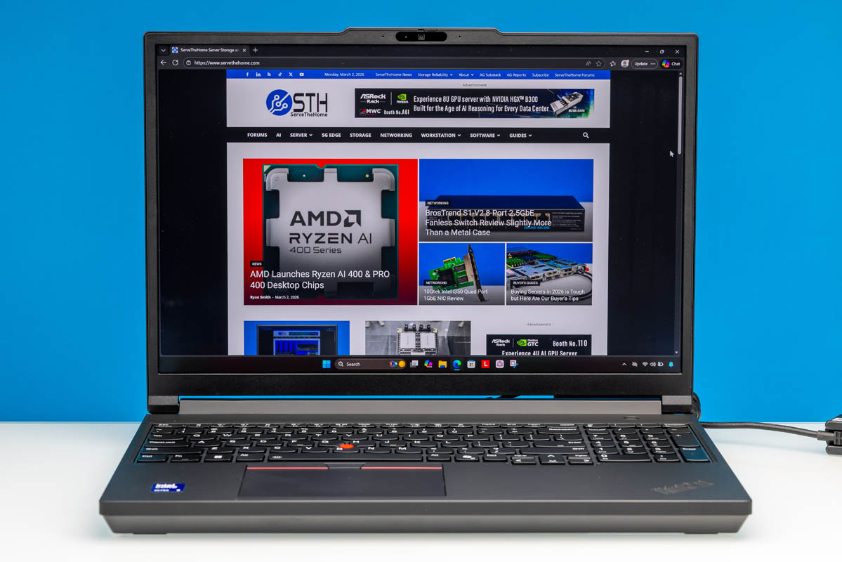
Lenovo Launches Powerful AI Workstation ThinkPad P16 Gen 3
