TSMC Expands Technology Roadmap with N2U and A12 Process
Key Takeaways
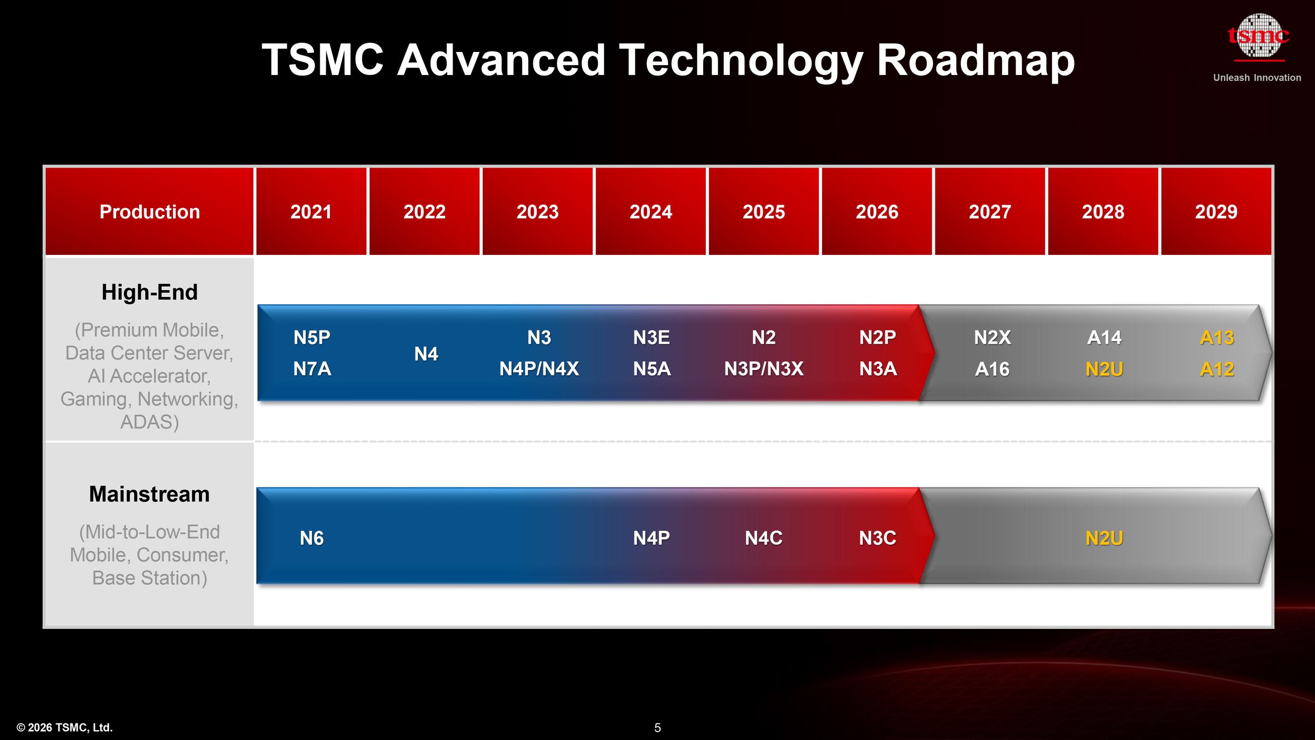
- 1TSMC announced new chip fabrication processes A12, A13, N2U for 2029.
- 2New strategy separates offerings for AI/HPC and consumer applications.
- 3Increases AI processing capabilities, reducing dependency on foreign tech.
TSMC unveiled its technology roadmap at the North American Technology Symposium, detailing its new fabrication processes A12 and A13, alongside the extended N2U. These nodes indicate a strategic shift as TSMC plans to produce advancements focused on applications like AI and High-Performance Computing (HPC). Notably, the roadmap lays out a clear path without incorporating High-NA EUV lithography nodes throughout 2029. TSMC’s latest technologies reflect a bifurcation in their development approach tailored for different markets, emphasizing AI’s growing dominance over traditional consumer segments.
This strategic pivot aims to bolster TSMC's output for demanding AI applications while ensuring that new nodes are introduced annually for client applications. The integration of Super Power Rail technology in the A12 and A16 models is pivotal, addressing power delivery constraints specific to AI workloads. This move could significantly enhance the capabilities of domestic AI infrastructures, fostering greater technology independence and potentially reducing reliance on foreign manufacturing expertise in high-tech domains.